
Power supply circuit design is necessary for any system development. If you are designing a board with an FPGA, you may need to install 5 or more switching regulators.
This article introduces the design procedure and verification method of the switching regulator, which is a little difficult.
-Switching regulator selection and circuit diagram
For example, assume that input VIN = 12(V) output VOUT = 3.3(V) load current IOUT = 4(A) is required.
Considering 80% derating, the loading current selects 5(A) product "= 4(A) / 80%".
From the requested specifications, we selected LT 8640.
Once you have decided which switching regulator to use, the first thing you need to check is the data sheet in English.
The Analog Devices datasheet contains many reference schematics.
Select a circuit diagram that meets the required specifications from the datasheet (Fig. 1).
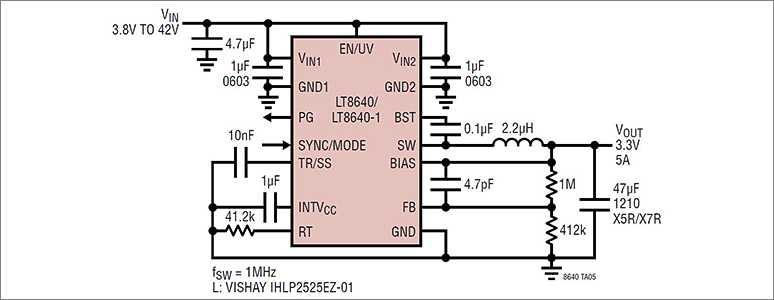
Fig. 1: LT8640 circuit diagram
- When there is no reference circuit of the required specification or confirmation of the peripheral constant
If you have a reference schematic, you can apply it to the actual circuit.
However, just in case, use the calculation formula in the application information section of the data sheet to check if the circuit constants are correct.
If there is no reference schematic, there are 2 design methods.
The first method is to design the circuit using the formula in the application information section of the datasheet.
The second way is to create a schematic using a LTPowerCAD from Analog Devices. It is also possible to design a compensation circuit by using LTPowerCAD.
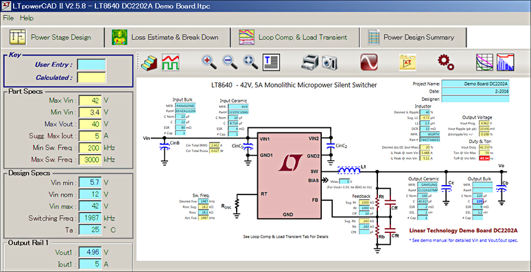
Fig. 2: LTPowerCAD
-Operation verification of switching regulator
Even if a circuit diagram is created, it is necessary to confirm whether actual noise performance and efficiency are expected.
It is recommended to obtain an evaluation board and check the operation of the tester on the actual machine.
Even with the same capacitor capacity, validation on a real machine is recommended, as the characteristics of the power supply will change depending on the manufacturer and the part number.
-How to verify the circuit before obtaining the demo board
It is best to verify with a demo board, but this can be a problem if it takes a long time to obtain or if you want to verify the schematics immediately.
In such cases, if you install LTspice, which is provided free by Analog Devices on your PC, you can use it for circuit verification.
You can find the LTspice demo circuit through below URL link.
If you verify the circuit on LTspice and couldn’t get the desired simulation results, there might be some problems with the circuit design.
In that case, it is recommended to check the circuit diagram to make sure that the connection is correct and that there is no difference in the setting of the peripheral constant.
-All depends on pattern design
You might want to say "design complete!" because the circuit diagram was completed and the result was as expected on LTspice, but the last pattern design (artwork) remains.
The performance of the switching regulator is determined by the pattern design.
Even if you copy and use Analog Devices's recommended schematics, or if you use a schematic that works with LTspice, you may encounter problems with incorrect pattern design, such as increased noise or the switching regulator not working (or in the worst case, broken).
To avoid such problems, check the following 2 points when designing a pattern.
- Follow the precautions in the recommended layout of the datasheet.
- Design based on the pattern layout information in the demo board design file.
The layout of the pattern in the datasheet may be described simply, so be sure to check the design information on the demo board.
Design information for LT8640 is available through below URL link.
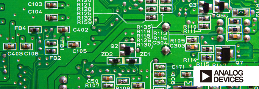
It is also very important that you do not leave the pattern design to the CAD staff but check again whether the pattern design is the same as the demo board.
If there is no problem so far, then wait for the completion of the board.